Researchers at MIT have developed a process that turns standard 300-millimetre silicon-photonics wafers into circuits that are both mechanically flexible and optically transparent. MIT News reported the work, led by Jelena Notaros with lead author Tal Sneh, on 3 September. It is published in Optica as “Transparent and mechanically-flexible wafer-scale silicon-photonics fabrication platform”.
Single photonic chips that are flexible, or transparent, have been made before, but not with a process that scales. “We’ve now developed a wafer-scale process that produces wafers that are mechanically flexible and optically transparent, enabling novel applications that weren’t previously possible with silicon photonics,” Notaros said.
How it is made
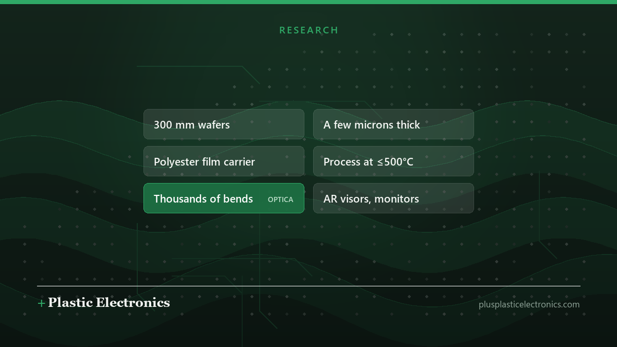
According to MIT News and Tech Xplore, the team starts with standard 300 mm silicon wafers and deposits and patterns optical waveguides as usual. A temporary rigid silicon support is then bonded on, and the original substrate is removed, leaving only ultrathin oxide and waveguide layers less than a tenth of the thickness of a human hair. A transparent polyester film is attached, and the temporary support is debonded. The finished structure is a few microns thick, and the process stays at or below 500°C.
The work was carried out with NY Creates at the Albany NanoTech Complex and with MIT.nano. Funding came from the US National Science Foundation, the Defense Advanced Research Projects Agency and a MathWorks Fellowship.
How far it bends
The chips were bent thousands of times without performance degradation and survived bending around cylinders as small as a screw, the reports say. Performance degraded only when they were bent repeatedly around a toothpick. Viewers saw minimal haze and no noticeable image distortion when looking through them. The summaries we read give no optical loss figures, transmission percentages or bend radius in millimetres. Those numbers will have to come from the paper, which we have not read in full.
Why it matters
Flexible electronics has largely been built from organic semiconductors, metal oxides and printed conductors precisely because silicon is rigid and opaque. A foundry process that keeps silicon photonics’ capabilities while shedding both properties widens the design space. The MIT team points to curved augmented-reality displays, pilot helmet visors and wearable health monitors that conform to the body. The choice of 300 mm wafers matters as much as the flexibility, because it keeps the work on the same class of tooling as commercial photonics.
What has not yet been shown is integration: light sources, detectors and electronic drive circuits on the same flexible, transparent carrier, and how the polyester film behaves across temperature and time.
What we’re watching
- Loss and transmission data from the Optica paper, compared with rigid silicon photonics.
- Demonstrations with integrated emitters or detectors rather than passive waveguides alone.
- Environmental and long-term stability of the polyester-backed stack.