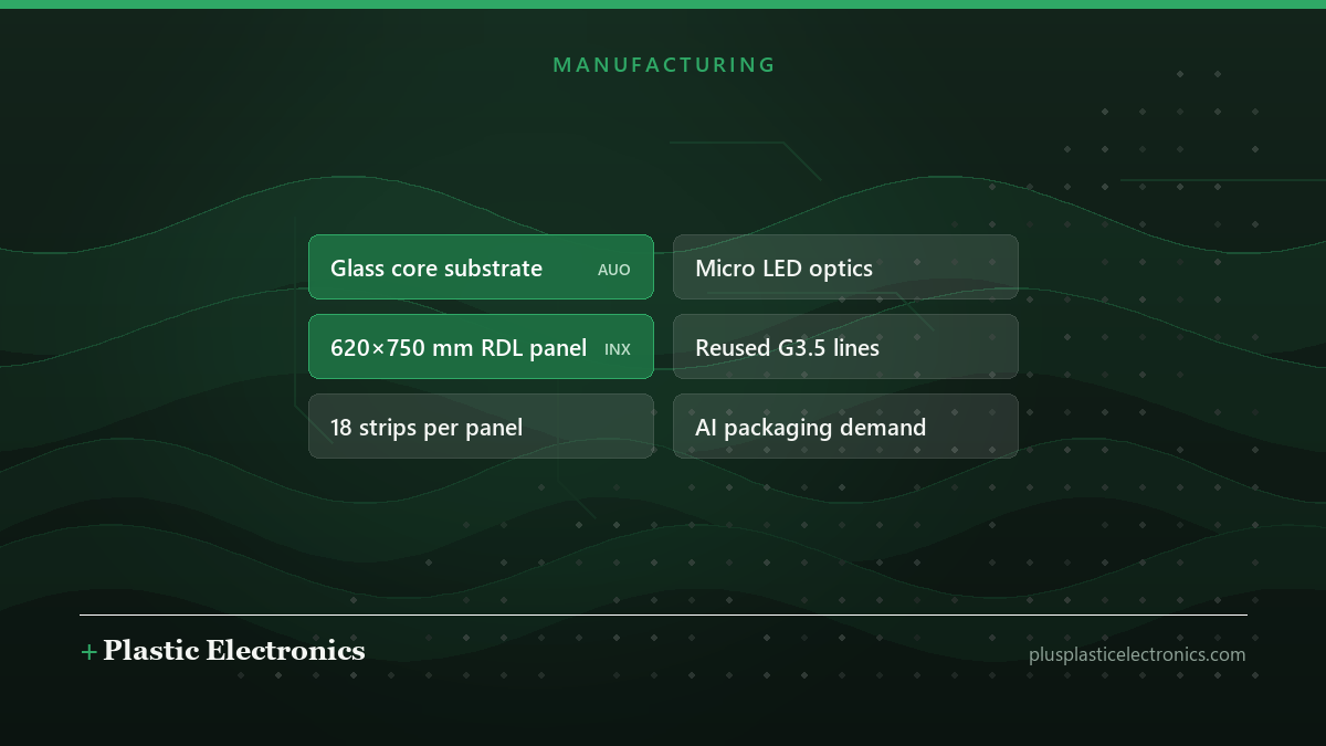
Two of Taiwan’s largest display makers used SEMICON Taiwan, held in Taipei from 2 to 4 September, to offer their glass-panel expertise as an answer to one of the chip industry’s tightest bottlenecks: packaging ever-larger AI processors. AUO showed glass core substrates built on Corning glass, alongside a micro LED co-packaged optics module. Innolux promoted what it calls the world’s largest redistribution-layer (RDL) substrate, made on revitalised G3.5 display lines.
AUO: from display glass to packaging substrates
According to AUO’s announcement, its glass core substrates combine Corning’s semiconductor-grade glass with AUO’s RDL process technology. The company cites a low coefficient of thermal expansion, high dimensional stability and low signal loss, and names AI, high-performance computing, high-bandwidth memory and co-packaged optics as target applications.
The second exhibit was optical. AUO’s micro LED co-packaged optics module targets high-speed interconnects of up to 10 metres in AI data centres, combining micro LED transmitters from Ennostar, photodetector receivers from Tyntek and photosensitive dielectrics from Daxin Materials. AUO quotes thermal stability to 125°C and an operating lifetime of more than 30,000 hours. “AI is driving demand for computing performance while redefining the value of optical communications,” said chief technology officer Wei-Lun Liao.
Innolux: an old line, a new product
Innolux’s SEMICON Taiwan exhibitor profile describes a 620 × 750 mm RDL substrate produced on existing G3.5 lines fitted with panel-level plating equipment. A single G3.5 substrate can be cut into 18 strips that fit standard flip-chip back-end packaging equipment, according to the profile. It claims finer line and space capability than ABF or BT substrates, a thinner profile and tighter die-to-die spacing. Innolux also describes panel-level testing that probes many sites across the whole panel at once.
For the flexible and printed electronics supply chain, the interesting part is the repurposing. Early-generation display fabs are long depreciated, and handling large glass substrates, plus patterning, deposition and plating across big rectangular panels, is exactly what they were built for. Panel-level packaging turns that legacy capacity into a potential route into semiconductors.
What is still unproven
Neither company disclosed customers, volumes or yields in the material we read, and the performance figures above are the companies’ own. DIGITIMES reported on 14 September that Taiwanese firms lead in fan-out panel-level packaging as overseas rivals race to catch up. That analysis is behind a paywall, and we have read only its summary. Panel warpage, overlay accuracy across large substrates and the long qualification cycles of chip customers remain the usual hurdles between an exhibition booth and production.
What we’re watching
- Named customer qualifications for Innolux’s RDL substrates or AUO’s glass core substrates.
- Whether other panel makers with idle early-generation lines announce similar conversions.
- Independent reliability data for the micro LED co-packaged optics module beyond AUO’s own lifetime figure.